Pc Ddr 266 Driver

ESIS: Compact PCs - Small Computers - Embeddable Fanless PC - Fanless Mini PC - Fanless Computer.
Glossary-Computer Motherboards-Computer Terms about PC Mainboard Mother Board Motherborad with great prices and best customer services.
DDR DIMM Computer Memory Module Description and pinout, Double Data Rate Memory.


- Download drivers for NVIDIA products including GeForce graphics cards, nForce motherboards, Quadro workstations, and more. Update your graphics card drivers today.
- Super Talent Technology is a leading Manufacturer of DDR DDR2 Value Memory for desktop computers and upgrades.
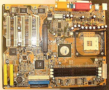
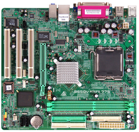
Motherboard
Dimensions / Mounting Holes / Chipset / Processor slot/socket
/ AGP / PCI / ISA / RAM / Port / Serial / Parallel / PS/2 / USB / VGA / SCSI / Jumper / Connector header / Jumper header
/ BIOS / Driver / Cable set
/ Processor / System RAM / Chassis / Power Supply / Socket 7 / Socket 8 / Slot
1 / Slot 2 / Xeon / Cache
/ L1 Cache / L2 Cache / ACPI
/ SOHO / ECP / EPP / ECC / APM / DMI / SDRAM
/ EDO / DIMM / SIMM
DDR3 SDRAM XMP DDR3L and DDR3U Dual Channel Triple Channel Quadruple-channel
Chipset Models
Intel 810 / Intel 440BX / Intel 440GX / Intel 440LX / Intel 440ZX / ALi 1541 / SiS
530 / SiS 600 / VIA Apollo Pro / Socket 1156 / Socket 1155 / Socket 1150 / Socket 1366 and Socket 2011
Form Factor
Baby AT BAT / ATX / MicroATX
Serial ATA / SATA 1.5 Gbit/s / SATA 3 Gbit/s / SATA 3.0 - 6 Gbit/s / eSATA / eSATAp / Mini-SATA mSATA / M.2 NGFF / SATA Express
List of motherboard manufacturers:
ASUS Biostar Gigabyte Technology Intel Jetway MSI Supermicro XFX Zotac EVGA Corporation
Motherboard - the principle printed circuit board
assembly in a computer; includes core logic chipset, interface sockets and/or slots, and
input/output I/O ports.
Printed circuit board PCB - a thin, laminated sheet composed of a series of epoxy
resin and copper layers and etched electronic circuits signal, ground and power
Chipset or core logic - two or more integrated circuits
which control the interfaces between the system processor, RAM, I/O devises, and adapter
cards.
Processor slot/socket - the slot or socket used
to mount the system processor on the motherboard
AGP - Accelerated Graphics Port - a high speed interface for
video cards; runs at 1X 66MHz, 2X 133MHz, or 4X 266MHz.
PCI - Peripheral Component Interconnect - a high speed interface
for video cards, sound cards, network interface cards, and modems; runs at 33MHz.
ISA - Industry Standard Architecture - a relatively low speed
interface primarily used for sound cards and modems; runs at approx. 8MHz.
RAM - Random Access Memory - see System RAM
Port serial, parallel, PS/2, USB, sound, LAN, VGA, SCSI -
interface connectors for the associated types of devices
Serial - a low speed interface typically used for mice and
external modems
Parallel - a low speed interface typically used for printers
PS/2 - a low speed interface used for mice and keyboards
USB - Universal Serial Bus - a medium speed interface typically
used for mice, keyboards, scanners, display panels control features, not data, speakers
control features, not sound, scanners, and some digital cameras.
USB 1.x
Released in January 1996, USB 1.0 specified data rates of 1.5 Mbit/s Low-Bandwidth and 12 Mbit/s Full-Bandwidth. It did not allow for extension cables or pass-through monitors, due to timing and power limitations. Few USB devices made it to the market until USB 1.1 was released in August 1998, fixing problems identified in 1.0, mostly related to using hubs. USB 1.1 was the earliest revision that was widely adopted.
USB 2.0
USB 2.0 was released in April 2000 now called Hi-Speed, adding higher maximum signaling rate of 480 Mbit/s due to bus access constraints the effective throughput is limited to 35 MB/s or 280 Mbit/s, in addition to the USB 1.x Full Speed signaling rate of 12 Mbit/s.
USB 3.0
USB 3.0 was released in November 2008. The standard defines a new SuperSpeed mode with a signaling speed of 5 Gbit/s and, due to encoding overhead, usable data rate of up to 4 Gbit/s 500 MB/s. A USB 3.0 port is usually colored blue, and is backwards compatible with USB 2.0.
USB 3.1
A January 2013 press release from the USB group revealed plans to update USB 3.0 to 10 Gbit/s, effectively putting it on par with Thunderbolt by mid-2013. The USB 3.1 specification was released on 31 July 2013, introducing a faster transfer mode called SuperSpeed USB 10 Gbps ; its logo features a Superspeed stylized as SUPERSPEED caption. The USB 3.1 standard increases the signalling rate to 10 Gbit/s, double that of USB 3.0, and reduces line encoding overhead to just 3 by changing the encoding scheme to 128b/132b. Though, some initial tests demonstrated usable transfer speeds of only 7.2 Gbit/s, suggesting a 30 overall overhead.
The USB 3.1 standard is backward compatible with USB 3.0 and USB 2.0. Using three power profiles of those defined in the USB Power Delivery Specification, it lets devices with larger energy demands request higher currents and supply voltages from compliant hosts - up to 2 A at 5 V for a power consumption of up to 10 W, and optionally up to 5 A at either 12 V 60 W or 20 V 100 W.
Short Cuts: USB Adp.,Cables Hubs Everything USB 2.0 Everything USB 3.0 How to install Front USB 2.0 How to install Front USB 3.0
VGA - Video Graphics Adapter - the interface from your video card
or integrated video connector and the system display monitor.
SCSI interface - Small Computer System Interface - the
interface between a SCSI controller and an external or internal SCSI device.
Jumper - a small block approx. 250 wide x. 312
long x. 125 thick with two holes running lengthwise which are connected with a metal
structure, or the functionally equivalent electronic interconnect ; used to
enable, disable, or select operating parameter on a motherboard or other PCB by
either electrically connecting two pins on the PCB closed or separating them open -
only one pin is covered or the jumper is removed.
Connector header - a series of two or more metal
pins on the motherboard or other PCB; used to attach a cable to indicator lights,
switches, and/or other devices in the computer
Jumper header - two pins or a series of two-pin groups
where jumpers are used.
BIOS - Pronounced bye-ose, an acronym for basic
input/output system. The BIOS is built-in software that determines what a computer can do
without accessing programs from a disk. On PCs, the BIOS contains all the code required to
control the keyboard, display screen, disk drives, serial communications, and a number of
miscellaneous functions.
The BIOS is typically placed in a ROM chip that comes with the computer it is often
called a ROM BIOS. This ensures that the BIOS will always be available and will not be
damaged by disk failures. It also makes it possible for a computer to boot itself. Because
RAM is faster than ROM, though, many computer manufacturers design systems so that the
BIOS is copied from ROM to RAM each time the computer is booted. This is known as
shadowing.
Many modern PCs have a flash BIOS, which means that the BIOS has been recorded on a flash
memory chip, which can be updated if necessary.
The PC BIOS is fairly standardized, so all PCs are similar at this level although there
are different BIOS versions. Additional DOS functions are usually added through software
modules. This means you can upgrade to a newer version of DOS without changing the BIOS.
PC BIOSes that can handle Plug-and-Play PnP devices are known as PnP BIOSes, or
PnP-aware BIOSes. These BIOSes are always implemented with flash memory rather than ROM.
Driver - software which defines the characteristics of a
device for use by another device or other software
Cable set - one or more interface cables typically, in
relation to a motherboard, includes cables for a floppy drive, hard drive, and CD-ROM
drive; may include cables between an internal connector header and a bracket or other
opening at the front of rear of the system; may include cables for both IDE/ATAPI and SCSI
devices.
Processor - the central processing unit CPU ;
the principle integrated circuit used for doing the computing in
personal computing
System RAM - the random access memory RAM used by the
CPU for computational purposes
Chassis - the structure used to house the various
internal components of the computer i.e., the motherboard, adapter cards,
various storage devices, power supply, etc. Normally called case.
Power Supply - the device used to convert, regulate, and
transmit external power for use by the components housed inside the computer chassis.
Socket 7 - The form factor for fifth-generation CPU chips
from Intel, Cyrix, and AMD. All Pentium chips, except Intel s Pentium Pro Socket 8 and
Pentium II Slot 1, conform to the Socket 7 specifications. Intel has decided to phase
out Socket 7 and replace it with Slot 1. But Intel s competitors, such as AMD and Cyrix,
are sticking with Socket 7, and are developing an enhanced version.
Socket 8 - The form factor for Intel s Pentium Pro
microprocessors. The Pentium Pro was the first microprocessor not to use the venerable
Socket 7 form factor. The Pentium II microprocessors use an even newer form factor called
Slot 1.
Socket 8 is a 387-pin ZIF socket with connections for the CPU and one or two SRAM dies for
the Level 2 L2 cache.
Slot 1 - The form factor for Intel s Pentium II processors.
The Slot 1 package replaces the Socket 7 and Socket 8 form factors used by previous
Pentium processors. Slot 1 is a 242-contact daughtercard slot that accepts a
microprocessor packaged as a Single Edge Contact SEC cartridge. A motherboard can have
one or two Slot 1s.
Slot 2 - A chip packaging design used in Intel s newer Pentium
II chipsets, starting with the Xeon CPU. While the Slot 1 interface features a 242-contact
connector, Slot 2 uses a somewhat wider 330-contact connector. The biggest difference
between Slot 1 and Slot 2, though, is that the Slot 2 design allows the CPU to communicate
with the L2 cache at the CPU s full clock speed. In contrast, Slot 1 only supports
communication between the L2 cache and CPU at half the CPU s clock speed.
Xeon - A line of Pentium II chipsets from Intel introduced in
1998. Unlike previous Pentium II chips, which used a Slot 1 form factor, Xeon chips use
Slot 2. This allows for faster data transfers between the CPU and L2 cache. Xeon chip
speeds start at 400 MHz.
Short Cuts: Motherboards by Interface
Back to Top
Cache - Pronounced cash, a special high-speed storage
mechanism. It can be either a reserved section of main memory or an independent high-speed
storage device. Two types of caching are commonly used in personal computers: memory
caching and disk caching.
A memory cache, sometimes called a cache store or RAM cache, is a portion of memory made
of high-speed static RAM SRAM instead of the slower and cheaper dynamic RAM DRAM used
for main memory. Memory caching is effective because most programs access the same data or
instructions over and over. By keeping as much of this information as possible in SRAM,
the computer avoids accessing the slower DRAM.
Some memory caches are built into the architecture of microprocessors. The Intel 80486
microprocessor, for example, contains an 8K memory cache, and the Pentium has a 16K cache.
Such internal caches are often called Level 1 L1 caches. Most modern PCs also come with
external cache memory, called Level 2 L2 caches. These caches sit between the CPU and
the DRAM. Like L1 caches, L2 caches are composed of SRAM but they are much larger.
Disk caching works under the same principle as memory caching, but instead of using
high-speed SRAM, a disk cache uses conventional main memory. The most recently accessed
data from the disk as well as adjacent sectors is stored in a memory buffer. When a
program needs to access data from the disk, it first checks the disk cache to see if the
data is there. Disk caching can dramatically improve the performance of applications,
because accessing a byte of data in RAM can be thousands of times faster than accessing a
byte on a hard disk.
When data is found in the cache, it is called a cache hit, and the effectiveness of a
cache is judged by its hit rate. Many cache systems use a technique known as smart
caching, in which the system can recognize certain types of frequently used data. The
strategies for determining which information should be kept in the cache constitute some
of the more interesting problems in computer science.
L1 Cache - Short for Level 1 cache, a memory cache built
into the microprocessor. See under cache. The L1 cache is also called the primary cache.
L2 Cache - Short for Level 2 cache, cache memory that is
external to the microprocessor. In general, L2 cache memory, also called the secondary
cache, resides on a separate chip from the microprocessor chip. The Pentium Pro, however,
has an L2 cache on the same chip as the microprocessor.
ACPI - Short for Advanced Configuration and Power Interface, a
power management specification developed by Intel, Microsoft, and Toshiba. ACPI, which
will be part of the next version of Windows, enables the operating system to control the
amount of power given to each device attached to the computer. With ACPI, the operating
system can turn off peripheral devices, such as a CD-ROM players, when they re not in use.
As another example, ACPI will enable manufacturers to produce computers that automatically
power up as soon as you touch the keyboard.
APM - Short for Advanced Power Management, an API developed by
Intel and Microsoft that allows developers to include power management in BIOSes. APM
defines a layer between the hardware and the operating system that effectively shields the
programmer from hardware details.
APM is expected to be gradually replaced by ACPI.
SOHO - Acronym for Small Office/Home Office, the fastest growing
market for computer hardware and software. So-called SOHO products are specifically
designed to meet the needs of professionals who work at home or in small offices.
ECP - Short for Extended Capabilities Port, a parallel-port
standard for PCs that supports bi-directional communication between the PC and attached
devices such as a printer. ECP is about 10 times faster than the older Centronics
standard.
Another modern parallel port for PCs that offers similar performance is the EPP Enhanced
Parallel Port.
EPP - Short for Enhanced Parallel Port, a parallel port standard
for PCs that supports bi-directional communication between the PC and attached devices
such as a printer. EPP is about 10 times faster than the older Centronics standard.
Another modern parallel port for PCs that offers similar performance is the ECP Extended
Capabilities Port.
ECC - Short for Error-Correcting Code memory, a type of memory
that includes special circuitry for testing the accuracy of data as it passes in and out
of memory.
DMI - Short for Desktop Management Interface, an API to enable
software to collect information about a computer environment. For example, using DMI a
program can determine what software and expansion boards are installed on a computer.
DMI is designed to be platform -independent and operating system -independent so that
programs can make the same function calls to collect information no matter what system
they re running in. This system independence is implemented by collecting information from
MIF files, which are plain text files containing information about a software or hardware
component.
DMI was designed by the Desktop Management Task Force DMTF, a consortium of hardware
manufacturers led by Intel. Version 2.0 allows a central computer not only to gather
information about computers connected to a network, but also to configure them. PCs that
comply with DMI 2.0 are sometimes called managed PCs.
SDRAM - Short for Synchronous DRAM, a new type of DRAM that can
run at much higher clock speeds than conventional memory. SDRAM actually synchronizes
itself with the CPU s bus and is capable of running at 100 MHz, about three times faster
than conventional FPM RAM, and about twice as fast EDO DRAM and BEDO DRAM. SDRAM is
replacing EDO DRAM in many newer computers
Today s fastest Pentium systems use CPU buses running at 100 MHz, so SDRAM can keep up
with them, though barely. Future PCs, however, are expected to have CPU buses running at
200 MHz or faster. SDRAM is not expected to support these high speeds which is why new
memory technologies, such as RDRAM and SLDRAM, are being developed.
EDO - Short for Extended Data Output Dynamic Random Access
Memory, a type of DRAM that is faster than conventional DRAM. Unlike conventional DRAM
which can only access one block of data at a time, EDO RAM can start fetching the next
block of memory at the same time that it sends the previous block to the CPU.
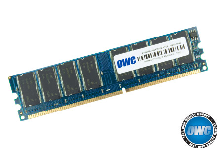
DIMM - Short for dual in-line memory module, a small circuit
board that holds memory chips. A single in-line memory module SIMM has a 32-bit path to
the memory chips whereas a DIMM has 64-bit path. Because the Pentium processor requires a
64-bit path to memory, you need to install SIMMs two at a time. With DIMMs, you can
install memory one DIMM at a time.
SIMM - Acronym for single in-line memory module, a small circuit
board that can hold a group of memory chips. Typically, SIMMs hold up 8 on Macintoshes
or 9 on PCs RAM chips. On PCs, the ninth chip is often used for parity error checking.
Unlike memory chips, SIMMs are measured in bytes rather than bits. SIMMs are easier to
install than individual memory chips.
The bus from a SIMM to the actual memory chips is 32 bits wide. A newer technology, called
dual in-line memory module DIMM, provides a 64-bit bus. For modern Pentium
microprocessors that have a 64-bit bus, you must use either DIMMs or pairs of SIMMs.
DDR3 SDRAM
In computing, DDR3 SDRAM, an abbreviation for double data rate type three synchronous dynamic random access memory, is a modern type of dynamic random access memory DRAM with a high bandwidth double data rate interface, and has been in use since 2007. It is the higher-speed successor to DDR and DDR2 and predecessor to DDR4 synchronous dynamic random access memory SDRAM chips. DDR3 SDRAM is neither forward nor backward compatible with any earlier type of random access memory RAM because of different signaling voltages, timings, and other factors.
DDR3 is a DRAM interface specification. The actual DRAM arrays that store the data are similar to earlier types, with similar performance.
The primary benefit of DDR3 SDRAM over its immediate predecessor, DDR2 SDRAM, is its ability to transfer data at twice the rate eight times the speed of its internal memory arrays, enabling higher bandwidth or peak data rates. With two transfers per cycle of a quadrupled clock signal, a 64-bit wide DDR3 module may achieve a transfer rate of up to 64 times the memory clock speed megahertz MHz in megabytes per second MB/s. With data being transferred 64 bits at a time per memory module, DDR3 SDRAM gives a transfer rate of memory clock rate x 4 for bus clock multiplier x 2 for data rate x 64 number of bits transferred / 8 number of bits/byte. Thus with a memory clock frequency of 100 MHz, DDR3 SDRAM gives a maximum transfer rate of 6400 MB/s. In addition, the DDR3 standard permits DRAM chip capacities of up to 8 Gbit.
XMP: Intel Corporation officially introduced the eXtreme Memory Profile XMP Specification on March 23, 2007 to enable enthusiast performance extensions to the traditional JEDEC SPD specifications for DDR3 SDRAM.
DDR3L and DDR3U: The DDR3L DDR3 Low Voltage standard is an addendum to the JESD79-3 DDR3 Memory Device Standard specifying low voltage devices. The DDR3L standard is 1.35V and has the label PC3L for its modules. Examples include DDR3L-800, DDR3L-1066, DDR3L-1333, and DDR3L-1600. The DDR3U standard is 1.25V and has the label PC3U for its modules.
On July 26, 2010, JEDEC Solid State Technology Association announced the publication of JEDEC DDR3L.
JEDEC standard modules:
Standard name
Memory clock
MHz
Cycle time
ns
I/O bus clock MHz
Data rate
MT/s
Module name
Peak transfer rate MB/s
Timings CL-tRCD-tRP
CAS latency ns
DDR3-800D
DDR3-800E
100
10
400
800
PC3-6400
6400
5-5-5
6-6-6
12
15
DDR3-1066E
DDR3-1066F
DDR3-1066G
133
7
533
1066
PC3-8500
8533
7-7-7
8-8-8
11
13
15
DDR3-1333F
DDR3-1333G
DDR3-1333H
DDR3-1333J
166
6
666
1333
PC3-10600
10666
9-9-9
10-10-10
12
DDR3-1600G
DDR3-1600H
DDR3-1600J
DDR3-1600K
200
5
1600
PC3-12800
12800
11-11-11
DDR3-1866J
DDR3-1866K
DDR3-1866L
DDR3-1866M
233
4
933
1866
PC3-14900
14933
12-12-12
13-13-13
DDR3-2133K
DDR3-2133L
DDR3-2133M
DDR3-2133N
266
3
2133
PC3-17000
17066
14-14-14
Dual Channel
Dual-channel-enabled memory controllers in a PC system architecture utilize two 64-bit data channels. Dual channel should not be confused with double data rate DDR, in which data exchange happens twice per DRAM clock. The two technologies are independent of each other and many motherboards use both, by using DDR memory in a dual-channel configuration.
Dual-channel architecture requires a dual-channel-capable motherboard and two or more DDR, DDR2 SDRAM, or DDR3 SDRAM memory modules. The memory modules are installed into matching banks, which are usually color-coded on the motherboard. These separate channels allow the memory controller access to each memory module. It is not required that identical modules be used if motherboard supports it, but this is often recommended for best dual-channel operation.
Triple Channel
DDR3 triple-channel architecture is used in the Intel Core i7-900 series the Intel Core i7-800 series only support up to dual-channel. The LGA 1366 platform e.g. Intel X58 supports DDR3 triple-channel, normally 1333 and 1600Mhz, but can run at higher clock speeds on certain motherboards. AMD Socket AM3 processors do not use the DDR3 triple-channel architecture but instead use dual-channel DDR3 memory. The same applies to the Intel Core i3, Core i5 and Core i7-800 series, which are used on the LGA 1156 platforms e.g., Intel P55. According to Intel, a Core i7 with DDR3 operating at 1066 MHz will offer peak data transfer rates of 25.6 GB/s when operating in triple-channel interleaved mode. This, Intel claims, leads to faster system performance as well as higher performance per watt.
When operating in triple-channel mode, memory latency is reduced due to interleaving, meaning that each module is accessed sequentially for smaller bits of data rather than completely filling up one module before accessing the next one. Data is spread amongst the modules in an alternating pattern, potentially tripling available memory bandwidth for the same amount of data, as opposed to storing it all on one module.
The architecture can only be used when all three, or a multiple of three, memory modules are identical in capacity and speed, and are placed in three-channel slots. When two memory modules are installed, the architecture will operate in dual-channel architecture mode.
Quadruple-channel
DDR3 Quadruple-channel architecture is used in the AMD G34 platform and the Intel LGA 2011 platform e.g., Intel X79. AMD processors which are used on the C32 platform instead use dual-channel DDR3 memory. Intel processors which are used on the LGA 1155 platform e.g., Intel Z68 instead use dual-channel DDR3 memory.
The architecture can only be used when all four, or a multiple of four, memory modules are identical in capacity and speed, and are placed in quad-channel slots. When two memory modules are installed, the architecture will operate in dual-channel architecture mode. When three memory modules are installed, the architecture will operate in triple-channel architecture mode.
Short Cuts: 2133MHz/PC3-17000 1866MHz/PC3-14900
1600MHz/PC3-12800 1333MHz/PC3-10600
1066MHz/PC3-8500 Dual Channel Triple Channel
Chipset Models - Today there are many chipset
models in the marketplace. The most popular for mainstream desktop computers are Intel s
810, BX, LX, and ZX. There are also third party chipsets available from Acer
Labs ALi, Silicon Integrated Systems SiS, and VIA Technologies VIA. The latter are
quite similar to their Intel counterparts but may add features not available in the Intel
chipsets. The third party chipsets may also support non-Intel processors like those from
AMD and others that have a 100MHz data bus and use the Socket 7
processor-to-motherboard socket. Intel also produces chipsets that support dual
processors. At the time this FAQ was prepared, only Intel was producing chipsets which
support multiple processors. The following are brief descriptions of the key features of
the most popular primary Intel and third party chipsets as of the date this FAQ was
prepared mid-June 99.
Intel 810 - Basic PC and Mainstream segments,
supports 2 DIMM max. 512MB, SDRAM only, ECC/parity not supported, integrated
direct AGP, integrated graphics controller enhanced i740, 66/100MHz data
bus, Ultra ATA/66 device support.
Intel 440BX - Performance segment, supports 4
DIMM max 1GB, SDRAM only, ECC/parity supported, AGP 2X, 66/100MHz data bus, Ultra
ATA/33 device support; dual processor support.
Intel 440GX - Workstation segment, supports 4
DIMM max 2GB, SDRAM only, ECC/parity supported, AGP 2X, 100MHz data bus, Ultra ATA/33
device support; dual processor support; supports Pentium II/III and Pentium Xeon II/III
slot 2.
Intel 440LX - Basic PC segment, supports 4
DIMM max 512MB SDRAM, 1GB EDO, ECC/parity supported, AGP 2X, 66MHz data bus, Ultra
ATA/33 device support; dual processor support
Intel 440ZX - Mainstream segment, supports 2
DIMM max 256MB, SDRAM only, ECC/parity not supported, AGP 2X, 66/100MHz data bus, Ultra
ATA/33 device support.
ALi 1541 - mainstream Socket 7, supports 3 DIMM, 100MHz
data bus, AGP 2X
SiS 530 - mainstream Socket 7, supports 3 DIMM, 100MHz data
bus, AGP 2X, integrated graphics controller
SiS 600 - mainstream Pentium II/III, supports 3 DIMM, 100MHz
VIA Apollo Pro - mainstream Pentium II/III, supports 4
DIMM, 100MHz data bus, AGP 2X
Intel 5/6/7/8/9 Series Chipset: Sandy Bridge chipsets 6 Series, Ivy Bridge chipsets 7 Series and Haswell chipsets 8 Series
The Nehalem microarchitecture moves the memory controller into the processor. For high-end Nehalem processors, the X58 IOH acts as a bridge from the QPI to PCI Express peripherals and DMI to the ICH10 southbridge. For mainstream and lower-end Nehalem processors, the integrated memory controller IMC is an entire northbridge some even having GPUs, and the PCH Platform Controller Hub acts as a southbridge.
Not listed below is the 3450 chipset see Xeon chipsets which is compatible with Nehalem mainstream and high-end processors but does not claim core iX-compatibility. With either a Core i5 or i3 processor, the 3400-series chipsets enable the ECC functionality of unbuffered ECC memory. Otherwise these chipsets do not enable unbuffered ECC functionality.
The Cougar Point Intel 6 series chipsets with stepping B2 were recalled due to a hardware bug that causes their 3 Gbit/s Serial ATA to degrade over time until they become unusable. Stepping B3 of the Intel 6 series chipsets will have the fix for this. The Z68 chipset which supports CPU overclocking and use of the integrated graphics does not have this hardware bug. The Z68 also added support for transparently caching hard disk data on to solid-state drives up to 64 GB, a technology called Smart Response Technology.
LGA 1156
Chipsets supporting LGA 1156 CPUs Lynnfield and Clarkdale.
Chipset
Code Name
sSpec Number
Bus Interface
Bus Speed
TDP
P55
Ibex Peak
SLH24 B3, SLGWV B2
DMI
2 GB/s
4.7 W
H55
5.2 W
H57
Q57
5.1 W
Short Cuts: Socket H LGA1156 Intel P55 Chipset Intel H55 Chipset Intel H57 Chipset Intel Q57 Chipset
LGA 1155
Chipsets supporting LGA 1155 CPUs Sandy Bridge and Ivy Bridge. The PCIe 2.0 lanes from the PCH ran at 5 GT/s in this series, unlike in the previous LGA 1156 chips..
H61
Cougar Point
SLH83 B2, SLJ4B B3
DMI 2.0
4 GB/s
6.1 W
P67
SLH84 B2 Recalled, SLJ4C B3
H67
SLH82 B2 Recalled, SLJ49 B3
Z68
SLJ4F B3
Q67
SLH85 B2, SLJ4D B3
Q65
SLH99 B2, SLJ4E B3
B65
SLH98 B2, SLJ4A B3
Z77
Panther Point
SLJC7 C1
6.7 W
Z75
SLJ87 C1
H77
SLJ88 C1
Q77
SLJ83 C1
Q75
SLJ84 C1
B75
SLJ85 C1
Short Cuts: Socket H LGA1156 Intel B75 Chipset Intel Q77 Chipset Intel H77 Chipset Intel Z75 Chipset Intel Z77 Chipset Intel B65 Chipset Intel Q67 Chipset Intel Z68 Chipset Intel H61 Intel H67 Intel P67
LGA 1150
Chipsets supporting the LGA 1150 CPUs are listed below. Haswell and Haswell Refresh CPUs are supported by all listed chipsets a BIOS update is usually required for Lynx Point motherboards to support Haswell Refresh CPUs, while the Broadwell CPUs are supported only by Z97 and H97 Wildcat Point chipsets.
Z87
Lynx Point
SR13A C1, SR176 C2
4.1 W
H87
SR139 C1, SR175 C2
H81
SR13B C1, SR177 C2
Q87
SR137 C1, SR173 C2
Q85
SR138 C1, SR174 C2
B85
SR13C C1, SR178 C2
Z97
Wildcat Point
SR1JJ
H97
SR1JK
Short Cuts: Socket H LGA1150 Intel Z97 Chipset Intel B85 Chipset Intel Q87 Chipset Intel H81 Chipset Intel H87 Chipset Intel Z87 Chipset
LGA 1366 LGA 2011
Chipsets supporting LGA 1366 and LGA 2011 CPUs.
X58 Northbridge
Tylersburg
SLGBT B2, SLGMX B3, SLH3M C2
QPI
Up to 12.8 GB/s
28.6 W
X79
Patsburg
SLJHW C0, SKJN7 C1
7.8 W
X99
Wellsburg
.
Short Cuts: Motherboard by Chipset Socket B LGA1366 Socket R LGA2011 Intel X58 Chipset Intel X79 Chipset
Form Factor - the physical layout of a motherboard in
regards the relative position of the adapter card expansion slots, the number of those
slots, the relative size of the motherboard, and the orientation of the board in the
chassis. For the purpose of this FAQ, only the Baby AT BAT, ATX, and MicroATX form
factors will be considered.
Baby AT BAT - this is the oldest of the currently available,
mainstream motherboard form factors. Its distinguishing features are its orientation in
the chassis the long axis goes from the back to the front of the chassis, the type of
keyboard connector typically referred to as a large DIN connector, the
presence of AT or PS/2 power supply connectors a series of 12 blades in one
or two adjacent male connectors, and the implementation of the various I/O connectors
serial and parallel ports via a bracket which goes into one of the adapter card slots at
the rear of the chassis. Please note that in some motherboards there may also be an ATX
power supply connector a rectangular grouping of 20 small sockets in two adjacent rows of
10.
ATX - this is the most common of today s mainstream motherboard
form factors. Its distinguishing features are its orientation in the chassis the long
axis goes from side-to-side at the rear of the chassis, the use of integrated I/O
connectors all the connectors are built into the motherboard and exit to the rear
of the chassis through an I/O shield where they are grouped together, and
only an ATX power supply connector is provided.
MicroATX - this is a variation of the ATX form factor. It is
much shorter in its long axis than the ATX and has fewer adapter card slots 3 compared to
the ATX with typically 7. Otherwise the features are the same as the ATX.
Short Cuts: Mini ITX Motherboards Micro ATX Motherboards
Motherboard Dimensions
- BTX 12.8 x 10.5 325 mm x 267 mm max
A standard proposed by Intel as a successor to ATX in the early 2000s, according to Intel the layout has better cooling. BTX Boards are flipped in comparison to ATX Boards, so a BTX or MicroBTX Board needs a BTX case, while an ATX style board fits in an ATX case.
The BTX form factor motherboards are incompatible with most of the ATX form factor cases and vice-versa. Moreover, cases such as the Cooler Master Series Stackers support a varying range of motherboard types such as ATX, BTX, Mini-ATX and so forth. However, all connectors are compatible, including power supplies, PCI cards, processors, RAM, hard drives, etc.
- MicroBTX or uBTX 10.4x10.5 264x267mm
- PicoBTX 8.0 x 10.5 in 203 x 267 mm max.
- EATX Extended ATX 12 x 13 305mm x 330 mm
Used in rackmount server systems. Typically used for server-class type motherboards with dual processors and too much circuitry for a standard ATX motherboard. The mounting hole pattern for the upper portion of the board matches ATX.
- ATX 12 x 9.6 305 mm x 244 mm
Created by Intel in 1995. As of 2007, it is the most popular form factor for commodity motherboards. Typical size is 9.6x12 although some companies extend that to 10x12.
- microATX 9.6 x 9.6 244 mm x 244 mm
A smaller variant of the ATX form factor about 25 shorter. Compatible with most ATX cases, but has fewer slots than ATX, for a smaller power supply unit. Very popular for desktop and small form factor computers as of 2007.
- FlexATX 9.0 x 7.5 228.6 x 190.5 mm max
It is a motherboard form factor derived from ATX. The specification was released in 1999 by Intel as an addendum to the microATX specification. It uses a subset of the motherboard mounting holes required for microATX and the same I/O plate system as ATX and microATX.
FlexATX specifies that a motherboard be no larger than 9.0 x 7.5 229 x 191 mm, and can have no more than 2 expansion slots.
- Mini-ATX 5.9 x 5.9 150 mm x 150 mm
Mini-ATX is slightly smaller than Mini-ITX. Mini-ATX motherboards were design with MoDT Mobile on Desktop Technology which adapt mobile CPU for lower power requirement and less heat generation, which makes them ideal for home theater PC HTPC and car PC for consumer and application PC for industrial.
- SSI CEB 12 x 10.5 305 mm x 267 mm
Created by the Server System Infrastructure SSI forum. Derived from the EEB and ATX specifications. This means that SSI CEB motherboards have the same mounting holes and the same IO connector area as ATX motherboards.
- Mini-ITX 6.7 x 6.7 170 mm x 170 mm max
A small, highly-integrated form factor, designed for small devices such as thin clients and set-top boxes.
- Nano-ITX 4.7 x 4.7 120 mm x 120 mm
Targeted at smart digital entertainment devices such as PVRs, set-top boxes, media centers and Car PCs, and thin devices.
- SSI CEB 12 x 10.5 in 305 x 267 mm
- SSI EEB 12 x 13 in 305 x 330 mm
Created by the Server System Infrastructure SSI forum. Derived from the EEB and ATX specifications. This means that SSI CEB motherboards have the same mounting holes and the same IO connector area as ATX motherboards, but SSI EEB motherboards do not.
- SSI MEB 16.2 x 13 in 411 x 330 mm
- Mobile-ITX2.953 x 1.772 in 75 x 45 mm
- DTX 200 x 244 mm max.
- Extended ATX EATX 12 x 13 in 305 x 330 mm
- Enhanced Extended ATX EEATX 13.68 x 13 in 347 x 330 mm
Used in rackmount server systems. Typically used for server-class type motherboards with dual processors and too much circuitry for a standard E.ATX motherboard.
Graphical comparison of physical sizes
Reference: WikipediA Computer form factor
FlexATX, microATX and ATX Mounting Holes:
Mounting Hole locations
Notes
FlexATX
B, C, F, H, J, S
MicroATX
B, C, F, H, J, L, M, R, S
Holes R and S were added for microATX form factor.
Hole B was defined in Full AT format
ATX
A C F G H J K L M
Hole F must be implemented in all ATX2.03-compliant chassis assemblies. The hole was optional in the ATX 1.1 specificatio.
dxy121109 ud081214dxy
Serial ATA - Serial ATA SATA is a computer bus interface that connects host bus adapters to mass storage devices such as hard disk drives and optical drives. Serial ATA replaces the older AT Attachment standard later referred to as Parallel ATA or PATA, offering several advantages over the older interface: reduced cable size and cost seven conductors instead of 40 or 80, native hot swapping, faster data transfer through higher signalling rates, and more efficient transfer through an optional I/O queuing protocol.
SATA host adapters and devices communicate via a high-speed serial cable over two pairs of conductors. In contrast, parallel ATA the redesignation for the legacy ATA specifications used a 16-bit wide data bus with many additional support and control signals, all operating at much lower frequency. To ensure backward compatibility with legacy ATA software and applications, SATA uses the same basic ATA and ATAPI command-set as legacy ATA devices.
SATA revision 1.0 - 1.5 Gbit/s - 150 MB/s
Revision 1.0a was released on January 7, 2003. First-generation SATA interfaces, now known as SATA 1.5 Gbit/s, communicate at a rate of 1.5 Gbit/s, and do not support Native Command Queuing NCQ. Taking 8b/10b encoding overhead into account, they have an actual uncoded transfer rate of 1.2 Gbit/s 150 MB/s. The theoretical burst throughput of SATA 1.5 Gbit/s is similar to that of PATA/133, but newer SATA devices offer enhancements such as NCQ, which improve performance in a multitasking environment.
During the initial period after SATA 1.5 Gbit/s finalization, adapter and drive manufacturers used a bridge chip to convert existing PATA designs for use with the SATA interface. Bridged drives have a SATA connector, may include either or both kinds of power connectors, and, in general, perform identically to their PATA equivalents. Most lack support for some SATA-specific features such as NCQ. Native SATA products quickly eclipsed bridged products with the introduction of the second generation of SATA drives.
As of April 2010 the fastest 10,000 RPM SATA mechanical hard disk drives could transfer data at maximum not average rates of up to 157 MB/s, which is beyond the capabilities of the older PATA/133 specification and also exceeds a SATA 1.5 Gbit/s link.
SATA revision 2.0 - 3 Gbit/s - 300 MB/s
Second generation SATA interfaces run with a native transfer rate of 3.0 Gbit/s, and taking 8b/10b encoding into account, the maximum uncoded transfer rate is 2.4 Gbit/s 300 MB/s. The theoretical burst throughput of SATA 3.0 Gbit/s is double that of SATA revision 1.0.
All SATA data cables meeting the SATA spec are rated for 3.0 Gbit/s and handle current mechanical drives without any loss of sustained and burst data transfer performance. However, high-performance flash drives can exceed the SATA 3 Gbit/s transfer rate; this is addressed with the SATA 6 Gbit/s interoperability standard.
SATA 3 Gbit/s is backward compatible with SATA 1.5 Gbit/s.
SATA revision 3.0 - 6 Gbit/s - 600 MB/s
Serial ATA International Organization presented the draft specification of SATA 6 Gbit/s physical layer in July 2008, and ratified its physical layer specification on August 18, 2008. The full 3.0 standard was released on May 27, 2009. It runs with a native transfer rate of 6.0 Gbit/s, and taking 8b/10b encoding into account, the maximum uncoded transfer rate is 4.8 Gbit/s 600 MB/s. The theoretical burst throughput of SATA 6.0 Gbit/s is double that of SATA revision 2.0. The 3.0 specification contains the following changes:
6 Gbit/s for scalable performance.
Continued compatibility with SAS, including SAS 6 Gbit/s. A SAS domain may support attachment to and control of unmodified SATA devices connected directly into the SAS domain using the Serial ATA Tunneled Protocol STP from the SATA_Revision_3_0_Gold specification.
Isochronous Native Command Queuing NCQ streaming command to enable isochronous quality of service data transfers for streaming digital content applications.
An NCQ Management feature that helps optimize performance by enabling host processing and management of outstanding NCQ commands.
Improved power management capabilities.
A small low insertion force LIF connector for more compact 1.8-inch storage devices.
A connector designed to accommodate 7 mm optical disk drives for thinner and lighter notebooks.
Alignment with the INCITS ATA8-ACS standard.
In general, the enhancements are aimed at improving quality of service for video streaming and high-priority interrupts. In addition, the standard continues to support distances up to one meter. The newer speeds may require higher power consumption for supporting chips, though improved process technologies and power management techniques may mitigate this. The later specification can use existing SATA cables and connectors, though it was reported in 2008 that some OEMs were expected to upgrade host connectors for the higher speeds.
The later standard is backward compatible with SATA 3 Gbit/s.
eSATA
Standardized in 2004, eSATA e standing for external provides a variant of SATA meant for external connectivity. It uses a more robust connector, longer shielded cables, and stricter but backward-compatible electrical standards. The protocol and logical signaling link/transport layers and above are identical to internal SATA. The differences are:
Minimum transmit amplitude increased: Range is 500 C600 mV instead of 400 C600 mV.
Minimum receive amplitude decreased: Range is 240 C600 mV instead of 325 C600 mV.
Maximum cable length increased to 2 metres 6.6 ft USB and FireWire allow longer distances.
The eSATA cable and connector is similar to the SATA 1.0a cable and connector, with these exceptions:
The eSATA connector is mechanically different to prevent unshielded internal cables from being used externally. The eSATA connector discards the L -shaped key and changes the position and size of the guides.
The eSATA insertion depth is deeper: 6.6 mm instead of 5 mm. The contact positions are also changed.
The eSATA cable has an extra shield to reduce EMI to FCC and CE requirements. Internal cables do not need the extra shield to satisfy EMI requirements because they are inside a shielded case.
The eSATA connector uses metal springs for shield contact and mechanical retention.
The eSATA connector has a design-life of 5,000 matings; the ordinary SATA connector is only specified for 50.
The eSATA version of SATA 6G operates at 6.0 Gbit/s the term SATA III is being avoided by the SATA-IO organization to prevent confusion with SATA II 3.0 Gbit/s, which was colloquially referred to as SATA 3G or SATA 300 since 1.5 Gbit/s SATA I and 1.5 Gbit/s SATA II were referred to as both SATA 1.5G or SATA 150.
eSATAp
eSATAp stands for powered eSATA. It is also known as Power over eSATA, Power eSATA, eSATA/USB Combo, or eSATA USB Hybrid Port EUHP. An eSATAp port combines the 4 pins of the USB 2.0 or earlier port, the 7 pins of the eSATA port, and optionally two 12-volt power pins. Both SATA traffic and device power are integrated in a single cable, as is the case with USB but not eSATA. Power at 5 volts is provided through two USB pins; power at 12 Volts may optionally be provided. Typically desktop, but not notebook, computers provide 12 volt power, so can power devices requiring this voltage, typically 3.5 disk and CD/DVD drives, in addition to 5 volt devices such as 2.5 drives.
Both USB and eSATA devices can be used with an eSATAp port, when plugged in with a USB or eSATA cable, respectively. An eSATA device cannot be powered via an eSATAp cable, but cables are available which make available both SATA or eSATA and power connectors from an eSATAp port.
An eSATAp connector can be built into a computer with internal SATA and USB, by fitting a bracket with connections for internal SATA, USB, and power connectors and an externally accessible eSATAp port. Though eSATAp connectors have been built into several devices, manufacturers do not refer to an official standard.
Mini-SATA mSATA
Mini-SATA abbreviated as mSATA, which is distinct from the micro connector, was announced by the Serial ATA International Organization on September 21, 2009. Applications include netbooks, laptops and other devices that require a solid-state drive in a small footprint.
The connector is similar in appearance to a PCI Express Mini Card interface, but is not electrically compatible; the data signals TX À/RX À SATA, PETn0 PETp0 PERn0 PERp0 PCI Express need a connection to the SATA host controller instead of the PCI Express host controller.
M.2 NGFF
M.2, formerly known as the Next Generation Form Factor NGFF, is a specification for computer expansion cards and associated connectors. It is intended to replace mSATA, which uses the PCI Express Mini Card physical layout. Having a smaller and more flexible physical specification, together with more advanced features, the M.2 is more suitable for solid-state storage applications in general, especially when used in small devices like ultrabooks or tablets.
The M.2 standard is designed as a revision and improvement to the mSATA standard, allowing for larger printed circuit boards PCBs to be manufactured. While mSATA took advantage of the existing PCI Express Mini Card form factor and connector, M.2 has been designed to maximize usage of the card space, while minimizing the footprint.
Supported host controller interfaces and internally provided ports are a superset to those defined by the SATA Express interface. Essentially, the M.2 standard is a small form factor implementation of the SATA Express interface, with the addition of an internal USB 3.0 port.
SATA Express
SATA Express, initially standardized in the SATA 3.2 specification, is an interface that supports either SATA or PCI Express storage devices. The host connector is backwards compatible with the standard 3.5-inch SATA data connector, allowing up to two legacy SATA devices to be connected. At the same time, host connector provides multiple PCI Express lanes as a pure PCI Express connection to the storage device.
Instead of the otherwise usual approach of doubling the native speed of the SATA interface, PCI Express was selected for achieving data transfer speeds greater than 6 Gbit/s. It was concluded that doubling the native SATA speed would take too much time, too many changes would be required to the SATA standard, and would result in a much greater power consumption when compared to the existing PCI Express bus.
In addition to supporting legacy Advanced Host Controller Interface AHCI, SATA Express also makes it possible for NVM Express NVMe to be used as the logical device interface for connected PCI Express storage devices.
Protocol
Short Cuts: SATA Hard Drives SATA II SATA 3.0Gb/s SATA III SATA 6.0Gb/s SCSI Hard Drives Solid State Drives SSD
ud081414dxy.
ASUS is a leading company driven by innovation and commitment to quality for products that include notebooks, netbooks, motherboards, graphics cards, displays.